How does a GPU work?
Overview
Historically, a Central Processing Unit (CPU) is a general purpose compute designed to handle a wide variety of tasks, optimized for sequential processing and overall system management. On the other hand, a GPU is a specialized compute designed for parallel processing, initially for graphics rendering but now widely used in various computationally intensive tasks, especially in machine learning and scientific computations.
Let’s take an example of large matrix multiplication on CPU & compare it against GPU:
1
2
3
4
5
6
7
8
9
10
11
12
13
14
15
16
17
18
19
20
21
22
23
24
25
import torch
import time

# Define matrix size
matrix_size = 10000

# Generate random matrices
A = torch.randn(matrix_size, matrix_size)
B = torch.randn(matrix_size, matrix_size)

# CPU computation
start_time = time.time()
C_cpu = torch.mm(A, B)
end_time = time.time()
print(f"CPU computation time: {end_time - start_time:.4f} seconds")

# Move matrices to GPU
A_gpu = A.to('cuda')
B_gpu = B.to('cuda')

# GPU computation
start_time = time.time()
C_gpu = torch.mm(A_gpu, B_gpu)
end_time = time.time()
print(f"GPU computation time: {end_time - start_time:.4f} seconds")
Upon running this code, you’ll notice the significant different in execution times (provided you have a GPU on your machine 😛)
1
2
CPU computation time: X.XXXX seconds
GPU computation time: Y.YYYY seconds
In this post, we will attempt to take a peek at the GPU’s internals to better understand how this specialized compute works. This helps us better understand the many GPU optimization techniques available in PyTorch like compile, quantization etc.
Benefits of GPUs
The Graphics Processing Unit (GPU) provides much higher instruction throughput and memory bandwidth than the CPU within a similar price and power envelope. Many applications leverage these higher capabilities to run faster on the GPU than on the CPU.
This difference in capabilities between the GPU and the CPU exists because they are designed with different goals in mind. While the CPU is designed to excel at executing a sequence of operations, called a thread, as fast as possible and can execute a few tens of these threads in parallel, the GPU is designed to excel at executing thousands of them in parallel.
The GPU is specialized for highly parallel computations and therefore designed such that more transistors are devoted to data processing rather than data caching and flow control as show in the diagram below.
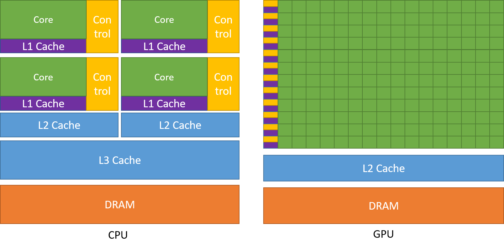 Devoting more transistors to data processing, for example, floating-point computations, is beneficial for highly parallel computations; the GPU can hide memory access latencies with computation, instead of relying on large data caches and complex flow control to avoid long memory access latencies, both of which are expensive in terms of transistors.
A GPU is currently not a standalone platform and must work in conjunction with a CPU. That’s why CPU is often referred to as the “host” and GPU as the “device”.
Hardware Comparison
| Component | Definition | CPU | GPU |
|---|---|---|---|
| Core | |||
| L1 Cache | The L1 cache is the smallest and fastest cache memory located directly on the processor chip. It is the first level of cache and has the lowest latency, meaning it can be accessed very quickly by the CPU. | Stores frequently accessed data and instructions to reduce the time the CPU spends fetching data from slower memory. Typically very small, ranging from 16 KB to 128 KB per core. | GPUs may have a small L1 cache per streaming multiprocessor (SM). Typically smaller compared to CPU L1 caches |
| L2 Cache | The L2 cache is larger than the L1 cache but slower. It acts as a secondary cache that holds data and instructions that the CPU/GPU might need next, which are not already in the L1 cache. | Generally ranges from 256 KB to 1 MB per core. Slower than L1 but faster than L3 cache. Serves as an intermediary between the fast L1 cache and the larger, slower L3 cache or main memory (DRAM). | Shared across multiple SMs, providing a larger cache to store data that might be reused across multiple threads. Larger than L1 but smaller than CPU L2 caches |
| L3 Cache | The L3 cache is a larger, shared cache that exists between the processor cores and the main memory. It is slower than L1 and L2 but larger and still faster than main memory. | Ranges from a few MBs to tens of MBs, shared across all cores of a processor. | If present, it serves similar purposes to CPU L3 caches but is less common. |
| Control Unit | The control unit is a component of the CPU/GPU that directs the operation of the processor. It interprets instructions from memory and converts them into signals that control other parts of the CPU/GPU. | Highly sophisticated, capable of handling complex instruction sets and multiple tasks. Manages the sequence of operations and handles branch prediction, instruction pipelining, and parallel execution. | Simpler and more distributed compared to CPUs. Each SM has its own control logic to manage the execution of threads. Focused on managing large numbers of parallel threads rather than complex sequential instruction execution. |
| DRAM | DRAM is a type of volatile memory used as the main memory in computers. It stores data that the CPU/GPU needs to access quickly, but unlike cache memory, it must be refreshed thousands of times per second. | Stores the bulk of data and instructions needed by the CPU during operation. Optimized for larger capacity. | Provides the necessary bandwidth to feed data to the many cores of the GPU. Higher bandwidth compared to traditional DDR memory used in CPUs, but with higher latency. |
CUDA
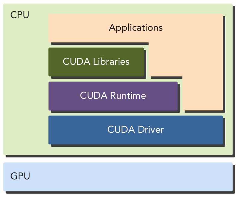
CUDA is a general-purpose parallel computing platform and programming model that leverages the parallel compute engine in NVIDIA GPUs to solve many complex computational problems in a more effi cient way. Using CUDA, you can access the GPU for computation, as has been traditionally done on the CPU.
CUDA provides two API levels for managing the GPU device and organizing threads:
- CUDA Driver API
- CUDA Runtime API
The driver API is a low-level API and is relatively hard to program, but it provides more control over how the GPU device is used. The runtime API is a higher-level API implemented on top of the Runtime API.
Nvidia GPU Architecture
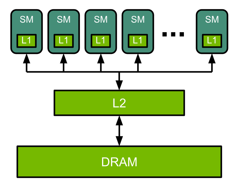
At a high level, NVIDIA® GPUs consist of a number of Streaming Multiprocessors (SMs), on-chip L2 cache, and high-bandwidth DRAM. Arithmetic and other instructions are executed by the SMs; data and code are accessed from DRAM via the L2 cache.
As an example, an NVIDIA A100 GPU contains 108 SMs, a 40 MB L2 cache, and up to 2039 GB/s bandwidth from 80 GB of HBM2 memory.
CUDA Cores
Essentially, it is the basic computational units within an NVIDIA GPU. Similar to CPU cores, but designed for parallel processing.
Threads on a CPU are generally heavyweight entities. The operating system must swap threads on and off CPU execution channels to provide multithreading capability. Context switches are slow and expensive. Threads on GPUs are extremely lightweight. In a typical system, thousands of threads are queued up for work. If the GPU must wait on one group of threads, it simply begins executing work on another.
CPU cores are designed to minimize latency for one or two threads at a time, whereas GPU cores are designed to handle a large number of concurrent, lightweight threads in order to maximize throughput.
Today, a CPU with four quad core processors can run only 16 threads concurrently, or 32 if the CPUs support hyper-threading. Modern NVIDIA GPUs can support up to 1,536 active threads concurrently per multiprocessor.
To manage such a large number of threads it uses a SIMT architecture.
Tensor Cores
Tensor Cores are specialized processing units found in NVIDIA GPUs, starting with the Volta architecture, designed specifically to accelerate tensor operations, which are fundamental to many machine learning and deep learning computations.
Training and inference of deep neural networks involve extensive matrix multiplications and tensor operations. Standard GPU cores, while highly parallel and efficient, still face performance limitations when handling large-scale matrix multiplications required in deep learning tasks.
A common operation in deep learning, such as matrix multiplication of the weights of neural networks with input data or other weight matrices, is computationally intensive. Performing these operations with traditional GPU cores can be slow and inefficient for the scale of data involved in modern deep learning applications.
Tensor Cores offer a specialized advantage over the CUDA cores due to the following reasons:
- Tensor Cores are designed to perform mixed-precision matrix multiplications and accumulations very efficiently. Tensor Cores use a mix of lower-precision (typically FP16) for intermediate calculations and higher-precision (FP32) for final accumulation to balance speed and accuracy.
- They operate on 4x4 matrix tiles, performing a fused multiply-add (FMA) operation in one cycle.
- They can perform multiple operations in a single cycle (such as multiply and accumulate) much more efficiently than general-purpose CUDA cores.
Before the introduction of Tensor Cores, NVIDIA GPUs did support lower precision operations like FP16, but the efficiency and performance gains were not as significant as what Tensor Cores can provide. Tensor Cores automate and optimize mixed precision operations, allowing developers to focus on model design rather than precision management.
Streaming Multiprocessor (SMs)
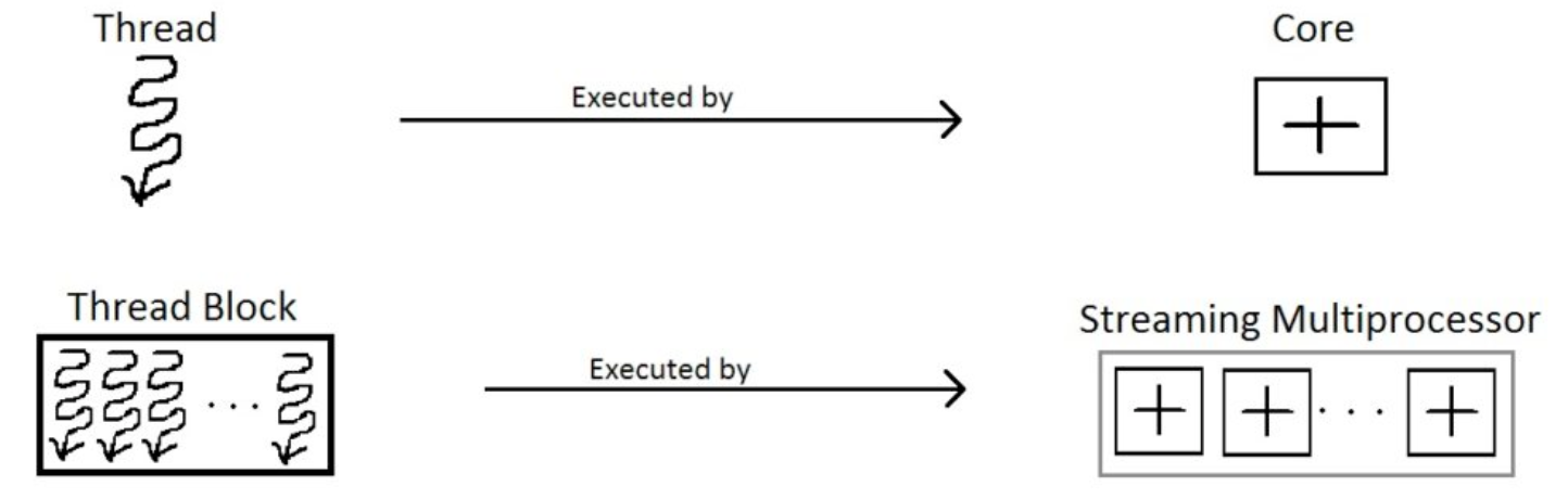
SMs are the primary building blocks of an NVIDIA GPU, containing multiple CUDA cores and other functional units. These are general purpose processors with a low clock rate target and a small cache.
Each SM in a GPU is designed to support concurrent execution of hundreds of threads, and there are generally multiple SMs per GPU, so it is possible to have thousands of threads executing concurrently on a single GPU.
SMs execute several thread blocks in parallel. As soon as one of its thread block has completed execution, it takes up the serially next thread block.
When a CUDA program on the host CPU invokes a kernel grid (task on GPU), the blocks of the grid (sub-tasks) are enumerated and distributed to multiprocessors with available execution capacity. The threads of a thread block execute concurrently on one multiprocessor, and multiple thread blocks can execute concurrently on one multiprocessor. As thread blocks terminate, new blocks are launched on the vacated multiprocessors.
Memory Hierarchy
CUDA-capable GPUs have a memory hierarchy as depicted in the figure below.
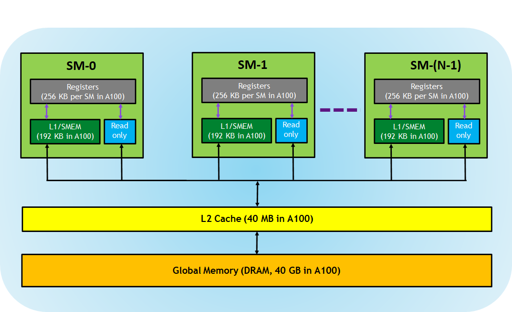
The following memories are exposed by the GPU architecture:
- Registers—These are private to each thread, which means that registers assigned to a thread are not visible to other threads. The compiler makes decisions about register utilization.
- L1/Shared memory (SMEM)—Every SM has a fast, on-chip scratchpad memory that can be used as L1 cache and shared memory. All threads in a CUDA block can share shared memory, and all CUDA blocks running on a given SM can share the physical memory resource provided by the SM..
- Read-only memory—Each SM has an instruction cache, constant memory, texture memory and RO cache, which is read-only to kernel code.
- L2 cache—The L2 cache is shared across all SMs, so every thread in every CUDA block can access this memory. The NVIDIA A100 GPU has increased the L2 cache size to 40 MB as compared to 6 MB in V100 GPUs.
- Global memory—This is the framebuffer size of the GPU and DRAM sitting in the GPU.
GPU Execution Model
As mentioned earlier, a GPU is NOT a standalone platform and works with CPU to execute any task. The diagram below captures the high-level interaction between a CPU & GPU while execution a task (on the GPU).
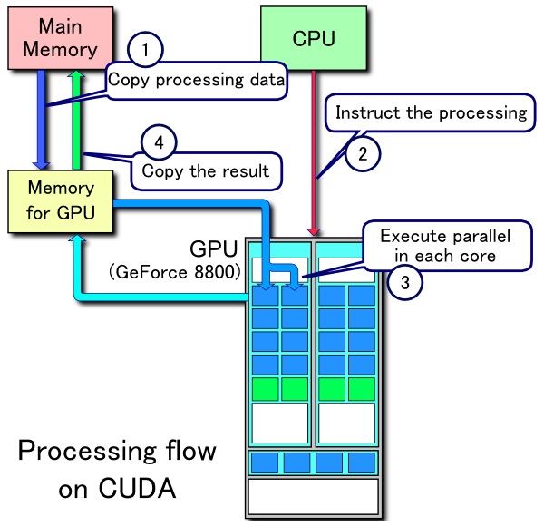
From the context of performance optimization, its important to profile that the time the task takes to move the data back and forth between CPU & GPU. Though the speeds are often in the range of 1900 Gbps, the GPU could process data sometimes even faster!
To broadly summarize the execution any CUDA program involves three main steps:
- Copy the input data from host memory to device memory, also known as host-to-device transfer.
- Load the GPU program and execute, caching data on-chip for performance.
- Copy the results from device memory to host memory, also called device-to-host transfer.
In this section, let’s look into the details of how an execution happens in the GPU.
CUDA Kernel & Thread Hierarchy
A task that needs to be executed on the GPU is called as a kernel. The kernel is typically a highly parallelizable function to leverage the GPU. For example, this can be simple function that multiplies two arrays elementwise. The kernel is passed from the host (CPU) to the device (GPU) where it gets broken down into a “grid” of “(CUDA) blocks” as shown below. 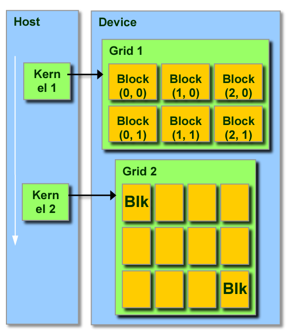
To simply we can say that a kernel can be broken down into identical units of operations. Each unit of operation can be acted upon by a single thread. A CUDA block is a group of threads that can execute a group of operations in a kernel. Taking the same example of elementwise multiplication, if the arrays are of length 10000, each CUDA block can be of 1000 threads where 1000 element multiplications will be performed. Within a thread block, the threads can cooperate and share memory.
Each thread and block have their own IDs which simplifies memory addressing when processing multi-dimensional data. As shown in the diagram below, block IDs can be 1D/2D and similarly for thread IDs. We can select whichever option that simplifies the execution.
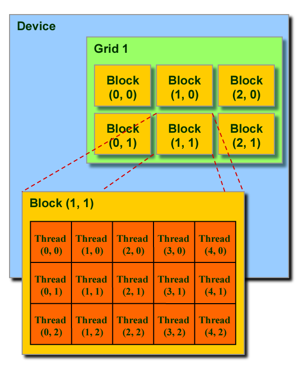
Connecting back our understanding of SMs and the memory hierarchy, every execution of a CUDA block in a SM can read/write within the hierarchy as shown below. 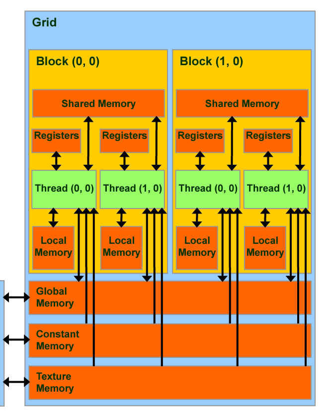
Each CUDA block is executed by one streaming multiprocessor (SM) and cannot be migrated to other SMs in GPU. One SM can run several concurrent CUDA blocks depending on the resources needed by CUDA blocks. Each kernel is executed on one device and CUDA supports running multiple kernels on a device at one time.
CUDA architecture limits the numbers of threads per block (1024 threads per block limit)
Hardware Execution
Now all this parallel processing in GPUs sounds great but how does it translate into the actual hardware! That happens with a combination of SIMT & Warp execution. Before we look into them, let’s understand SIMD which precedes SIMT.
Single Instruction, Multiple Data (SIMD)
SIMD is a parallel programming architecture where a single instruction is used to operate on multiple data points simultaneously. SIMD is often integrated right into the hardware design. For example, imagine you have a list of numbers and you want to add 2 to each number. Using SIMD, a single “add 2” instruction is applied to several numbers at once.
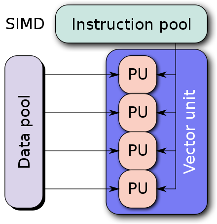
SIMD machines exploit data level parallelism but not concurrency: there are simultaneous (parallel) computations, but each unit performs the exact same instruction at any given moment (just with different data).
Let’s take our example to understand this better. Let’s say our SIMD machine can process 8 units at a time in parallel. We are passing an array of size 10 and asking it to “add 2” to every element.
- SIMD reads 8 elements, adds 2 and returns
- SIMD reads 2 elements, adds 2 and returns
Now let’s add a bit more complexity and say “add 2” to every element and “mul by 2”.
- SIMD reads 8 elements, adds 2 and returns
- SIMD reads 2 elements, adds 2 and returns
- SIMD reads 8 elements, multiplies 2 and returns
- SIMD reads 2 elements, multiplies 2 and returns
This what we mean by SIMD exploits data parallelism but not concurrency. SIMD processing units are bound by hardware to perform the same instructions. This means in task #2, there are 6 units in the SIMD that are idle!
Single Instruction, Multiple Threads (SIMT)
SIMT is a parallel programming architecture that essentially combines SIMD with multi-threading so that it can take advantage of both data parallelism and concurrency. Each thread can process different data independently but executes the same instruction as shown in the memory hierarchy earlier.
When a CUDA program on the host CPU invokes a kernel grid, the blocks of the grid are enumerated and distributed to SMs with available execution capacity. The threads of a thread block execute concurrently on one SM, and multiple thread blocks can execute concurrently on one SM. As thread blocks terminate, new blocks are launched on the vacated multiprocessors.
A SM is designed to execute hundreds of threads concurrently. To manage such a large number of threads, it employs the SIMT architecture. The instructions are pipelined, leveraging instruction-level parallelism within a single thread, as well as extensive thread-level parallelism through simultaneous hardware multithreading.
SIMD and SIMT are really two perspectives on the same concept. In both cases the hardware is designed to efficiently run an operation on many data elements simultaneously. The SIMT approach of CUDA is mostly a different software view on the same hardware where you mask the execution lane.
Warp Execution
Warps are the basic unit of execution in an SM. When you launch a grid of thread blocks, the thread blocks in the grid are distributed among SMs. Once a thread block is scheduled to an SM, threads in the thread block are further partitioned into warps. A warp consists of 32 consecutive threads and all threads in a warp are executed in Single Instruction Multiple Thread (SIMT) fashion; that is, all threads execute the same instruction, and each thread carries out that operation on its own private data.
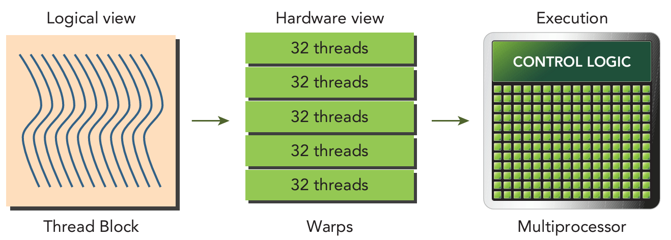
The hardware always allocates a discrete number of warps for a thread block. A warp is never split between different thread blocks. If thread block size is not an even multiple of warp size, some threads in the last warp are left inactive.
Warp Divergence
Control fl ow is one of the fundamental constructs in any high-level programming language. GPUs support traditional, C-style, explicit flow-control constructs, such as if…then…else, for, and while.
CPUs include complex hardware to perform branch prediction, that is, to predict at each conditional check which branch an application’s control flow will take (Speculative/Predictive Execution). If the prediction is correct, branching on CPUs incurs only a small performance penalty.
GPUs are comparatively simple devices without complex branch prediction mechanisms. Because all threads in a warp must execute identical instructions on the same cycle, if one thread executes an instruction, all threads in the warp must execute that instruction. This could become a problem if threads in the same warp take different paths through an application. For example, consider the following statement:
1
2
3
4
if cond:
  ...
else:
  ...
Suppose for 16 threads in a warp executing this code, cond is true, but for the other 16 cond is false. Threads in the same warp executing different instructions is referred to as warp divergence.
If threads of a warp diverge, the warp serially executes each branch path, disabling threads that do not take that path. Warp divergence can cause significantly degraded performance. To obtain the best performance, you should avoid different execution paths within the same warp.
Understanding the GPU specs
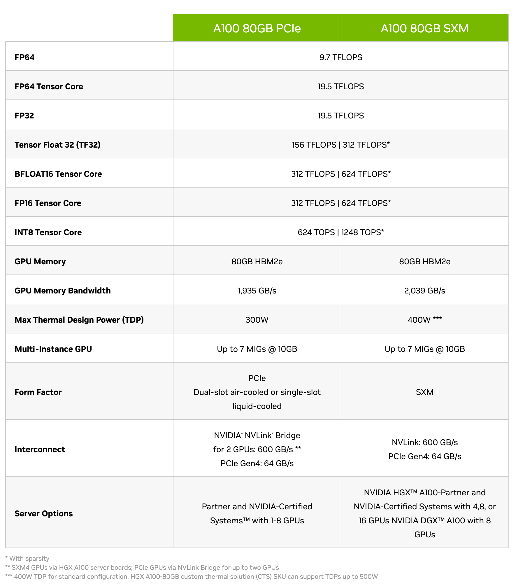
TFLOPS stands for “trillion floating-point operations per second.” It is a metric used to measure the computational performance of a computer system, particularly its ability to perform floating-point arithmetic operations which is the core metric for ML operations.
FP64, FP32, FP16 etc refer to the precision of the data. As the precision decreases you can see that the TFLOPS increase quite rapidly. Lot of optimizations happen at lower precision due to specialized tensor cores as mentioned earlier.
Large GPU memory capacity allows for handling larger datasets and more complex models, which is beneficial for ML engineers working with PyTorch. Sometimes the model can inherently be large or maybe we want to pass larger batches to the model to drive up utilization.
High memory bandwidth is essential for efficiently feeding data to the GPU during training and inference, especially for large neural networks.
The A100 GPU incorporates various features introduced with the NVIDIA Ampere architecture, such as Multi-Instance GPU (MIG), NVLink, and NVSwitch. Features like NVLink and NVSwitch enable multi-GPU setups for scaling PyTorch training across multiple GPUs. MIG allows for partitioning a single GPU into multiple instances, enabling efficient resource utilization in cloud environments.
Further Readings
- https://developer.nvidia.com/blog/tag/cuda-refresher/
- https://docs.nvidia.com/deeplearning/performance/dl-performance-gpu-background/index.html
- https://docs.nvidia.com/cuda/cuda-c-programming-guide/index.html#
- https://www.youtube.com/watch?v=QQceTDjA4f4&ab_channel=ChristopherHollinworth
- https://en.wikipedia.org/wiki/Single_instruction,_multiple_data
- https://blog.paperspace.com/understanding-tensor-cores/
- Book - CUDA C Programming
- Book - Programming Massively Parallel Processors